Electricity and electronics: State and apply principles and components used in electronics
Unit 2: Semi-conductors
Leigh Kleynhans
Unit 2 outcomes
By the end of this unit you will be able to:
- Describe semiconductors.
- Identify intrinsic properties and doping – properties by design.
- Describe principles of the p–n junction.
What you should know
Before you start this unit, make sure you can:
- Explain the structure of the atom. Refer to level 2 subject outcome 5.2 unit 1 if you need help with this.
- Work with the properties of elements and their arrangement in the periodic table. Refer to level 2 subject outcome 5.3 units 1, 2 and 3 if you need help with this.
- Define the principles of bonding. Refer to level 2 subject outcome 5.4 unit 3 if you need help with this.
Introduction
The classification of substances would be easy if they could be divided simply into conductors and insulators. However, if this was the case, we wouldn’t be able to make computers, CD players, cell phones, iPods and many other things which are part of modern life. The operation of modern technological devices is based on substances that are classified as semiconductors. Semiconductors are defined by their unique electric conductive behaviour, somewhere between that of a conductor and an insulator.
Atomic structure of semiconductors
To understand how semiconductors work, you must understand how electrons are organised in an atom. You should remember from previous physical science levels that the electrons in an atom are organised in or energy levels. The outermost shell is called the .
Metals tend to be good conductors of electricity because they usually have ‘free electrons’ in their valence shells that can move easily between atoms, and electricity involves the flow of electrons.
In insulators, the electrons in the valence shell are the ones that form bonds with neighbouring atoms. These bonds are called , and the electrons cannot move freely.
Carbon, silicon, and germanium have a unique property in their electron structure – each has four electrons in its outer shell. It is possible for all the valence electrons to be shared between adjacent atoms and the atoms arrange themselves into structures called crystals. Semiconductors are made of these crystals, usually silicon crystals.
In figure 1, each circle represents a silicon atom, and the lines between the atoms represent the shared electrons. Each of the four valence electrons in each silicon atom is shared with one adjacent silicon atom. Thus, each silicon atom is bonded with four other silicon atoms.
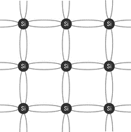
Pure silicon crystals are not useful electronically. There are no ‘free electrons’, so it is an insulator. However, under certain conditions the crystal can conduct electricity.
Extrinsic semiconductors
The process of deliberately introducing other elements into a crystal is called doping. The element introduced by doping is called a dopant. By carefully controlling the doping process and the dopants that are used, silicon crystals can transform into one of two distinct types of conductors:
- n-type semiconductor
- p-type semiconductors.
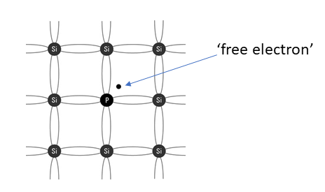
An n-type semiconductor is created when the dopant is an element that has five electrons in its valence layer. Phosphorus is commonly used for this purpose. The phosphorus atoms join the crystal structure of the silicon, each one bonding with four adjacent silicon atoms just like a silicon atom would. Because the phosphorus atom has five electrons in its valence shell, but only four of them are bonded to adjacent silicon atoms, the fifth valence electron is left unbonded. These extra valence electrons in the phosphorous atoms start to behave like the ‘free’ valence electrons in a regular conductor such as copper and the doped silicon can conduct electricity. Because this type of semiconductor has extra electrons (which are negatively charged), it is called an n-type semiconductor.
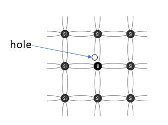
A p-type semiconductor is created when the dopant (such as boron) has only three electrons in the valence shell. When a small amount is incorporated into the crystal, the atom can bond with four silicon atoms, but since it has only three electrons to offer, a hole is created. The hole is a vacant ‘space’ which behaves like a positive charge (attracting electrons to it), so semiconductors doped in this way are called p-type semiconductors.
Like a positive charge, holes attract electrons. But when an electron moves into a hole, the electron leaves a new hole at its previous location. Thus, in a p-type semiconductor, holes are constantly moving around within the crystal as electrons constantly try to fill them up.
A minute amount of either n-type or p-type doping turns a silicon crystal from a good insulator into a viable (but not great) conductor – hence the name ‘semiconductor’. When voltage is applied to either an n-type or a p-type semiconductor, current flows, for the same reason that it flows in a regular conductor: the negative side of the voltage pushes electrons, and the positive side pulls them. The result is that the random electron and hole movement that is always present in a doped semiconductor becomes organised in one direction, creating measurable electric current.
Principles of p-n junctions
N-type and p-type silicon are not that amazing by themselves; but when you put them together, you get some interesting behaviour at the junction. This arrangement is called a p-n junction and is the basis of electronic components called diodes.
A diode is the simplest possible semiconductor device. A diode allows current to flow in one direction but not the other. You may have seen turnstiles at a stadium or a station that let people go through in only one direction. A diode is a one-way turnstile for electrons. When you put n-type and p-type silicon together as shown in figure 4, you get an interesting phenomenon that gives a diode its unique properties.
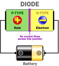
Even though n-type silicon by itself is a conductor, and p-type silicon by itself is also a conductor, the combination shown in figure 4 does not conduct any electricity. The negative electrons in the n-type silicon get attracted to the positive terminal of the battery. The positive holes in the p-type silicon get attracted to the negative terminal of the battery. No current flows across the junction because the holes and the electrons are each moving in the wrong direction. This arrangement is referred to as . If you flip the battery around, the diode will conduct electricity. The free electrons in the n-type silicon are repelled by the negative terminal of the battery.

The holes in the p-type silicon are repelled by the positive terminal. At the junction between the p-type and n-type silicon, holes and free electrons meet. The electrons fill the holes. Those holes and free electrons cease to exist, and new holes and electrons spring up to take their place. The effect is that current flows through the junction. This arrangement is referred to as . This property of diodes, which allows current to flow only if they are placed in a circuit in a forward biased position, make them the electronic version of a valve. The application of this property in electronic devices will be covered in the next unit.
Intrinsic semiconductors
Intrinsic semiconductors do not contain any impurities. They will be insulators as there are no free electrons to conduct electricity. However, if the substance is heated, electrons that are involved in covalent bonds can become ‘excited’ and free themselves from the bond. This creates free electrons (negative charge carriers) and creates holes in the position they left (positive charged areas). In this way a pure semiconductor can start to conduct electricity when connected to a voltage source.
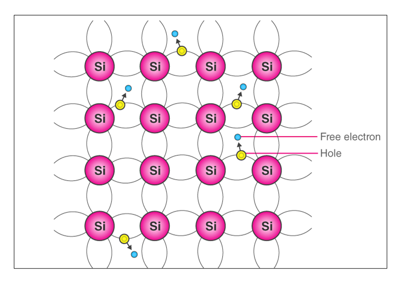
The semiconductor will only conduct electricity when heated and will become an insulator when it cools down.
Summary
In this unit you have learnt the following:
- Semiconductors are elements that have four valence electrons forming covalent bonds between the atoms forming a crystal.
- Extrinsic semiconductors are formed by introducing small amounts of another element in a process called doping. This allows it to conduct electricity.
- If a dopant with five valence electrons is used, the semiconductor is called an n-type semiconductor.
- If a dopant with three valence electrons is used, the semiconductor is called a p-type semiconductor.
- Diodes are constructed by joining a p-type semiconductor to an n-type semiconductor called a p-n junction.
- Diodes allow current to flow in a circuit only when they are connected in the forward biased direction.
- Intrinsic semiconductors can only conduct electricity when they have been heated and electrons in covalent bonds become free, leaving behind positive holes.
Unit 2: Assessment
Suggested time to complete: 20 minutes
- Explain why elements that form semiconductors have a crystalline structure.
- Name two substances that are classified as semiconductors.
- Give one word for the following:
- the process of adding impurities to create a semiconductor.
- substances that can be used for the process in question 3 a).
- Explain the difference between an n-type and a p-type semiconductor.
- State whether the following would be an n-type or p-type semiconductor:
- germanium doped with boron
- silicon doped with phosphorus
- germanium doped with aluminium
- silicon doped with arsenic
- .
- Name the electronic component that consists of a p-n junction.
- State how this component needs to be connected in a circuit to allow current to flow.
- Explain how intrinsic semiconductors allow current to flow.
The full solutions are at the end of the unit.
Unit 2: Solutions
Unit 2: Assessment
- They have four valence electrons so will form four covalent bonds with surrounding atoms in a symmetrical lattice pattern.
- silicon, germanium.
- .
- doping
- dopant
- An n-type semiconductor has been doped with an element with five valence electrons creating ‘free electrons’ not involved in covalent bonds with surrounding atoms. These electrons will be the charge carriers when connected to a voltage source.
A p-type semiconductor has been doped with an element with three valence electrons, creating positive holes where there is an unpaired electron. These positive holes act as charge carriers as they attract electrons towards them when connected to a voltage source. - .
- p-type (boron has three valence electrons)
- n-type (phosphorus has five valence electrons)
- p-type (aluminium has three valence electrons)
- n-type (arsenic has five valence electrons)
- .
- diode
- The side of the diode with the p-type semiconductor must be connected to the positive terminal of the power source and the side with the n-type semiconductor must be connected to the negative terminal of the power source. This is forward biased.
- Intrinsic semiconductors do not have free electrons but heating them will cause electrons in covalent bonds to become free. They can then become charge carriers at this higher temperature and conduct electricity.
Media Attributions
- img01_Figure1 © L Kleynhans is licensed under a CC BY (Attribution) license
- img02_Figure2 © L Kleynhans is licensed under a CC BY (Attribution) license
- img03_Figure3 © L Kleynhans is licensed under a CC BY (Attribution) license
- img04_Figure4 © L Kleynhans is licensed under a CC BY (Attribution) license
- img05_Figure5 © L Kleynhans is licensed under a CC BY (Attribution) license
- img06_Figure6 © L Kleynhans is licensed under a CC BY (Attribution) license
the energy levels around the nucleus of an atom where the electrons are found
the outermost shell or energy level of an atom containing the electrons that are involved in bonding
when a pair of electrons is shared between two atoms
when the p-type semiconductor of a diode is connected to the negative terminal of the battery and the n-type is connected to the positive terminal and current cannot flow
when the p-type semiconductor of a diode is connected to the positive terminal of the battery and the n-type is connected to the negative terminal allowing current to flow
